
Soitec Deep Dive
Soitec (SLOIF/SOI.PA): the Sole Qualified Supplier of the Substrate Beneath the AI Optical Transition, and a Market Still Pricing a Smartphone Parts Supplier

Introduction

Every time you ask an AI chatbot a question, data moves. It flows between thousands of GPUs packed into racks, between racks packed into clusters, between clusters connected across data center floors. That data used to travel on copper wires. It can’t anymore. The speed and power demands of modern AI have hit a physical wall: copper wires simply cannot move enough data fast enough without burning too much electricity. The industry’s answer is light. Silicon photonics chips convert electrical signals into light, send them through tiny channels carved into silicon, and transmit data over fiber at far higher speeds and lower power than copper can manage.
Those silicon photonics chips are built on a specific type of wafer: a layered structure of silicon, glass-like oxide, and a thin crystal film that forms the channels through which light travels. That wafer is called Photonics-SOI. Several companies make general-purpose SOI wafers: Shin-Etsu, GlobalWafers, SUMCO, and others. But for the specific photonics-grade SOI that the major chip factories have tested, approved, and are now scaling for AI data center production, there is today only one qualified volume supplier.
That company is Soitec.
Soitec doesn’t make chips. It doesn’t design them. It makes the specialty wafers that chip factories use to build their circuits on. Think of the relationship like a steel mill and a car factory: the car factory gets the credit, but without the right grade of steel, the car doesn’t work.
These aren’t ordinary silicon wafers you can buy from any supplier. They are multi-layer structures built using Soitec’s proprietary Smart Cut process, a technique that uses charged particles and molecular bonding to transfer ultra-thin crystal layers with precision measured in atoms. This process has been refined over the past 30 years. It’s protected by more than 4,300 active patents. In fact, Soitec was ranked among the top patent filers in France by INPI, and the company files roughly 2 patents per day worldwide across Asia, Europe, and the United States. Behind each filing, their R&D, technology, and IP teams work together to turn ideas into protected innovations that directly feed the company’s competitive advantage and negotiating power in global markets.
If Nvidia designs the engine and TSMC assembles the car, Soitec supplies the specialty steel used to forge the chassis.
These wafers are tested and approved by chip factories over a 12 to 24-month qualification process. Once approved, switching to a different wafer supplier means the chip factory has to retest everything, risking billions in production yield. The switching costs aren’t just theoretical. They’re built into how the entire industry works.
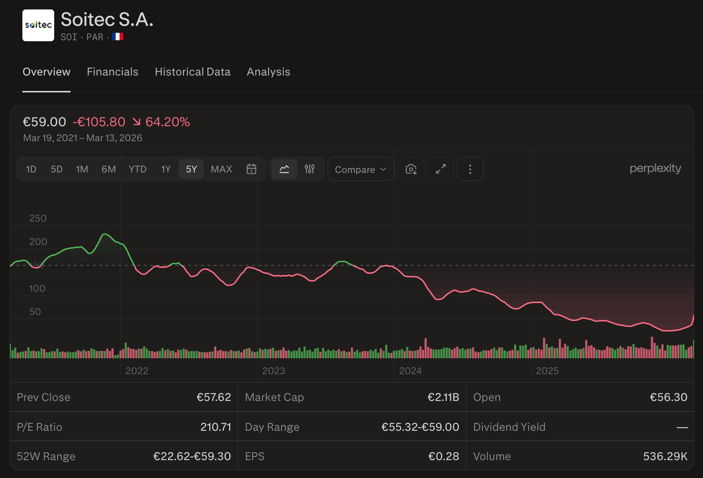
The market prices Soitec as a regular semiconductor supplier stuck in a downturn. It trades at roughly €57 per share, giving it an enterprise value of about €2.2 billion. Every Wall Street analyst covering it rates it Hold. The consensus price target is €33. The stock is down over 70% from its 2021 peak above €200.
My view: the market is looking at the downturn and missing the transformation happening underneath it. Soitec is not a cyclical smartphone parts company. It is the dominant substrate supplier underpinning AI optical interconnects, 5G/6G communications, and the shift from copper to light, with €1.1 billion in factory capacity already built and ready to be filled.
Why Soitec Exists: The Physics Problem
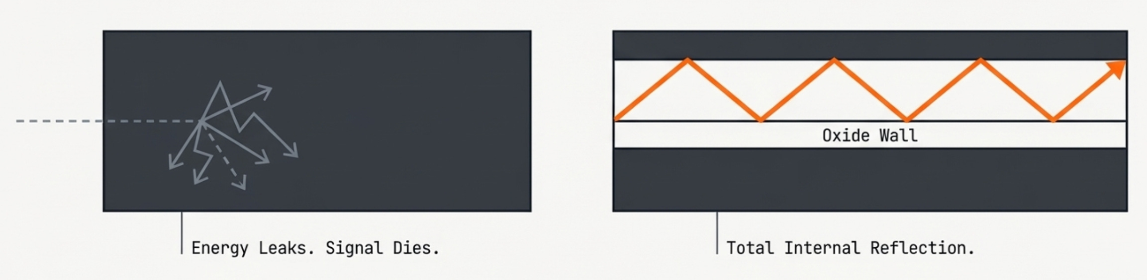
As chips get smaller and power demands grow, especially for AI workloads, regular silicon hits physical limits. Electrical current leaks. Energy is wasted as heat. Signals degrade. In a standard chip, the transistor sits directly on top of a conducting layer, and the interference between the two causes problems that get worse as you shrink the transistor.
SOI (Silicon on Insulator) wafers fix this by placing a thin glass-like insulating layer between the transistor and the base wafer. This insulating layer acts like a wall, blocking interference, reducing power leakage, and letting the transistor run faster and cooler.
In silicon photonics, the insulating layer performs a function that is even more critical. It acts as a cladding that traps light within tiny channels carved into the silicon, just as the coating on a fiber-optic cable prevents light from escaping. Without that insulating layer, there’s no light channel. Without the light channel, there’s no silicon photonics chip. Without the chip, there’s no high-speed optical link for AI data centers.
Other materials can also handle light. Indium phosphide (InP) is used for lasers, silicon nitride works for certain passive functions, and hybrid approaches combine multiple materials. These all serve real markets. But for the mainstream, high-volume silicon photonics chips that Tower Semiconductor, GlobalFoundries, and TSMC are building for data center transceivers, SOI is the platform they’ve all chosen, because it combines optical performance with standard chip-making compatibility at costs and scales the alternatives can’t match.
Why the Chip Factories Can’t Just Make Their Own Wafers
So why don’t TSMC or Samsung just make their own specialty wafers? Three reasons, all structural.
First, Soitec’s Smart Cut process is proprietary and protected by a thicket of 4,300+ patents that cover not just the core technique but also every important variation and improvement developed over three decades.
Second, the process knowledge (the exact temperatures, pressures, chemical treatments, and hundreds of other settings that determine whether a production run works or produces scrap) exists as institutional know-how inside Soitec’s teams in France and Singapore. It’s not written in any textbook. It can’t be copied from a finished wafer.
Third, any new supplier would face a chicken-and-egg problem. To sell wafers, you need chip factories to approve you. To get approved, you need a track record of producing high-quality wafers at scale. To make good wafers at volume, you need years of production data. There’s no shortcut.
The strongest proof that the IP holds up: in October 2023, Soitec terminated its Smart Cut license with GlobalWafers, the world’s third-largest silicon wafer maker. GlobalWafers sued. In July 2025, they settled, with a transition period through June 2027. After that, GlobalWafers is out. The fact that Soitec pulled the license from a major global player and won the legal fight tells you the IP is enforceable and Soitec holds the cards.
Smart Cut: How It Works
Smart Cut works like a precision cutting tool at the atomic level. Charged particles (hydrogen or helium ions) are injected into a silicon crystal at a specific depth, creating a weak point within it. That crystal is then bonded face-to-face to a second wafer that already has an oxide layer. When heat is applied, the crystal splits along the weak point, transferring an ultra-thin layer (sometimes just a few dozen atoms thick) onto the second wafer. The leftover donor wafer is recycled and reused.
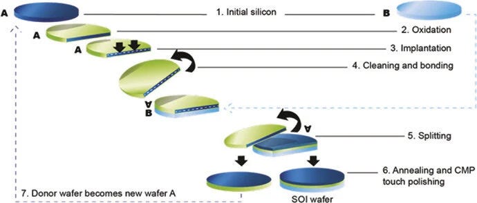
The result is a sandwich, a thin crystal film on top, an insulating oxide layer in the middle, and a thick base wafer on the bottom, all bonded at the molecular level with thickness control measured in angstroms (tenths of a billionth of a meter).

The closest comparison in the chip industry is ASML’s position in EUV lithography, though the parallel has limits. ASML has 100% of the EUV market, with a supply chain that can’t be physically copied. Soitec has about 60-70% of the broader SOI wafer market, with licensees and smaller producers active in less demanding segments. For photonics-grade SOI specifically, Soitec’s position is much closer to ASML’s. But the broader SOI market is a concentrated group of a few players, not a pure one-company show.
The Licensing Picture
Bears worry about Soitec’s licensing relationships. Here’s the context.
Shin-Etsu has held a Smart Cut license since 1997, renewed in 2012. The license lets Shin-Etsu operate the technology on its own, but it’s specifically scoped: no sublicensing, no technology transfer, and Shin-Etsu gets the process version from the license date, not the latest improvements. Shin-Etsu remains a secondary SOI producer, not a competitive threat.
GlobalWafers had its license terminated and lost the legal fight, as described above.
Simgui, owned by China’s NSIG, was licensed in 2014 for 200mm wafers only. The setup is tightly controlled: Simgui makes the wafers, Soitec manages the sales worldwide. On March 13, 2026, Soitec and NSIG agreed to extend this arrangement for 10 more years, with no new technology transfer and a joint commitment to strengthen Soitec’s patents in China.
The key takeaway: for photonics-grade SOI, where all the growth is, the licensing question doesn’t apply. Neither Shin-Etsu nor GlobalWafers can make photonics-grade wafers at volume. Soitec is the only qualified supplier in the segment that matters most.
The Product Lineup
Soitec runs five established products and several early-stage technologies. Together, they reveal a company that isn’t just a one-product business but a platform that gets more valuable as the chip industry gets more complex.
RF-SOI is the cash cow: the dominant wafer for 5G radio-frequency chips with roughly 70%+ global market share. Every 5G phone uses one. This product line is in the middle of an inventory correction (detailed later), which is the main reason revenue is depressed right now. Customer inventories stood at about 2 million wafers at the end of December 2025, being worked down by 200,000-300,000 per quarter toward a target of 1 million by March 2027.
FD-SOI (Fully Depleted SOI) is for ultra-low-power, high-performance chips. It’s the only wafer technology that can put a 5G mmWave radio into a single chip. Design wins are confirmed in premium iPhones (mmWave), Android flagships (Wi-Fi 7), and Starlink satellites (an 18nm processor for advanced computing in orbit). FD-SOI also provides 150 times the resistance to hardware hacking compared to regular silicon, making it critical for automotive cybersecurity as cars become software-defined. GlobalFoundries runs its 22nm FD-SOI process on Soitec wafers, and UMC has a partnership for 3D RF-SOI targeting 5G. The FAMES project, backed by €830 million in EU funding and inaugurated in January 2026, is developing next-generation FD-SOI at 7nm and below, which would push Soitec’s platform into entirely new computing territories.
POI (Piezoelectric on Insulator) is used for advanced RF filters and is quickly becoming the industry standard. As of early 2026, 13 customers are in production, and 12 more are in testing. On March 4, 2026, Skyworks announced a multi-year deal to use Soitec’s POI wafers for its Sky5 5G platform. POI content per phone is growing from about 4 mm2 to 11 mm2 as 5G spectrum becomes more crowded and phones need more sophisticated filtering.
Photonics-SOI is the growth engine, as detailed in the next section.
Power-SOI serves the automotive and industrial power management markets.
Among the newer technologies, three stand out. SmartSiC (silicon carbide for EVs) took a €41 million write-down in H1 FY26 after Chinese competitors crashed prices. This is a real miss and a reminder that not every Soitec bet pays off. LNOI (Lithium Niobate on Insulator) targets the fastest data speeds (1.6T-3.2T) where silicon photonics alone can’t keep up, and Soitec is one of the only companies positioned to supply both LNOI and Photonics-SOI from the same technology base. And GaN-on-Silicon (gallium nitride) recently hit a major milestone: Soitec and NTU Singapore demonstrated over 50% power efficiency at FR3 frequency bands, positioning it for 6G base stations and next-generation wireless infrastructure.
The AI and Photonics Opportunity
If Soitec were just an RF-SOI company going through a temporary downturn, the story would be a straightforward recovery play. What makes it bigger is the Photonics-SOI business.
The Problem: AI Data Centers Need More Bandwidth Than Copper Can Deliver
AI clusters are getting enormous, with hundreds of thousands of GPUs working together. The data moving between those GPUs needs to travel fast and efficiently. Copper wires worked fine at lower speeds, but at 800 gigabits per second and beyond, they hit physical limits on distance, power consumption, and bandwidth. The solution is silicon photonics: chips that use light instead of electricity.
McKinsey projects data center power demand to nearly triple to 219 GW by 2030. AI data center spending is growing at over 20% per year toward roughly $830 billion by 2030. Optical interconnect sales are projected to grow from about $10 billion in 2024 to roughly $40 billion by 2030. The number of optical links per GPU is scaling from 128 today to potentially millions in future designs.
The Progression: Optical Gets Closer to the Chip Over Time
Right now, optical links connect data centers and server racks. Over the next few years, optical moves inside the rack (co-packaged optics, estimated 2027-2028), then eventually inside the chip package itself (beyond 2030). Each step closer to the chip means more Photonics-SOI per server.
Soitec’s Position
The broader SOI market has multiple suppliers. But photonics-grade SOI requires very specific layer thicknesses, surface quality, and oxide properties that go beyond standard SOI specs. These specs have to be individually qualified with each chip factory. As of today, Soitec is the only supplier that has been approved for volume photonics-grade SOI production by the major silicon photonics foundries: Tower Semiconductor, GlobalFoundries, and TSMC.
Could a competitor eventually get approved too? Yes. The question is whether that takes 2 years or 5, and whether Soitec uses that time to extend its lead. As the photonics market grows, foundries will eventually push for a second supplier. But today, every photonics chip Tower ships maps to a Soitec wafer order.
Tower committed $920 million in silicon photonics capital spending, with over 70% of that capacity spoken for by customers before it was even built. Tower is 5x-ing its photonics capacity from year-end 2025 to year-end 2026. TSMC’s COUPE silicon photonics packaging technology enters production in H2 2026. AAOI booked a $200 million+ order for 1.6T transceivers. NVIDIA invested $4 billion in Lumentum and Coherent to lock down optical component supply.
Management guides 20-30% annual growth for Photonics-SOI from a roughly €100 million base in FY26. Morgan Stanley models 35% growth for FY27. Edge and Cloud AI (the division that houses photonics) grew 34% organically in H1 FY26, while the overall company shrank 29%.
The Feynman Scenario
NVIDIA’s Feynman architecture, the successor to Rubin targeting around 2028, appears to integrate silicon photonics directly into the GPU package, according to supply chain reports. If this ships as described, it would be a major shift, silicon photonics moving from network switches into the processor itself.
We deliberately exclude this from our base case because the exact timing and scope are unconfirmed. But if Feynman integrates photonics, each GPU would need its own photonics wafer, potentially multiplying demand by orders of magnitude versus today’s transceiver-based model. NVIDIA’s $4 billion investment in downstream optical suppliers suggests the company is serious about this direction. The upstream wafer supplier, Soitec, remains unprotected by any comparable strategic investment at a fraction of those companies’ valuations. Treat this as a bull-case option, not a certainty.
Where Soitec Sits in the Supply Chain
It helps to trace the full chain. At the top, hyperscalers (Microsoft, Google, Amazon, Meta, Oracle) are spending $660-690 billion combined on AI data center buildout in 2025-2026. That flows into chip designers (Nvidia, AMD, Intel), then into network equipment (Arista, Ciena), then into optical transceivers and engines (AAOI, Lumentum, Coherent), then into chip packaging (BE Semi, Fabrinet, Amkor), then into foundries (Tower, GlobalFoundries, TSMC, UMC), and finally into substrates and materials at the very bottom: Soitec for SOI wafers, AXT and Sumitomo for compound semiconductor substrates.
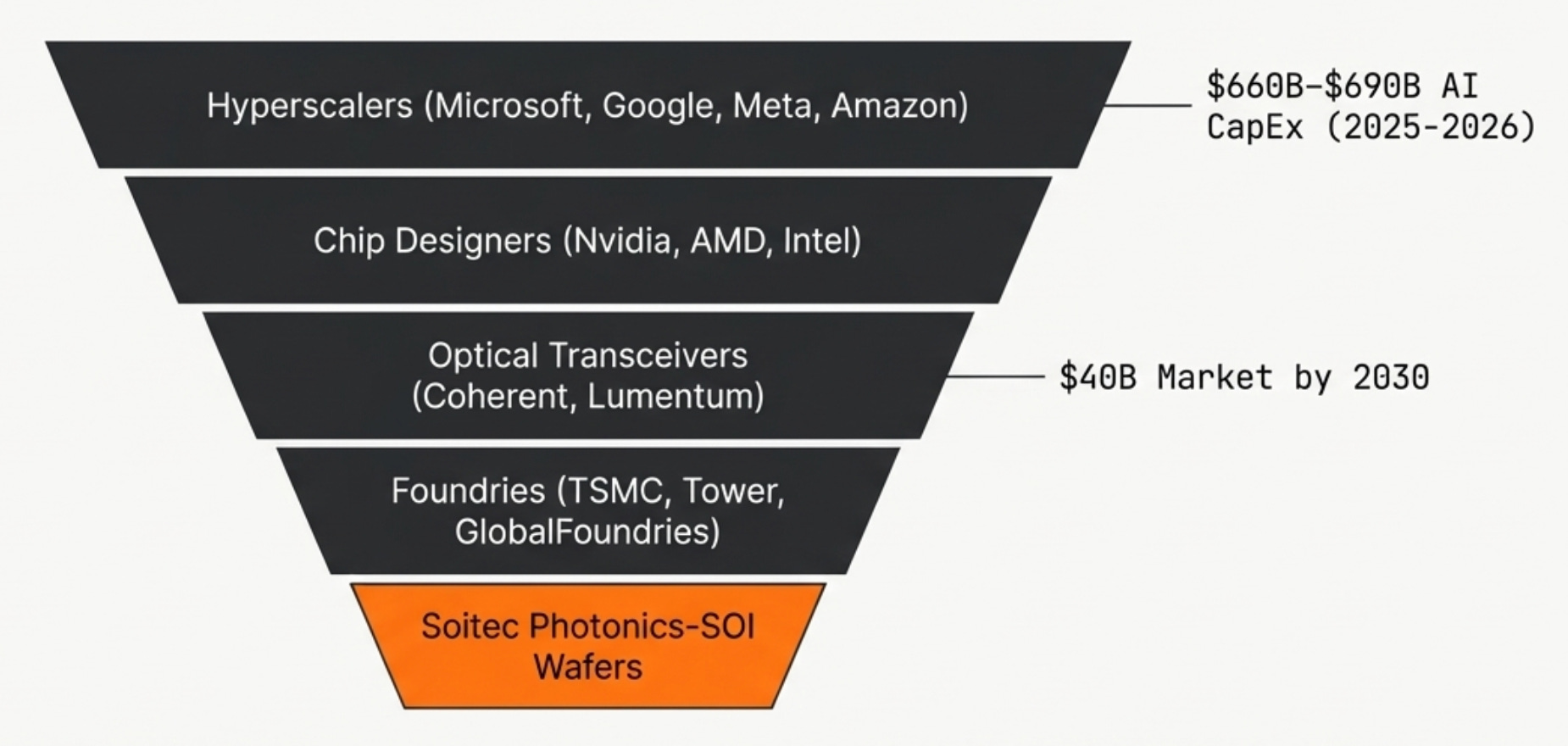
Soitec sits at the bottom of a 12-layer stack. Optical networking is about 5-8% of total AI data center spending. The substrate layer is a fraction of that.
But the investment case isn’t about capturing a big percentage of the $40 billion optical market. It’s about being the irreplaceable input at the base of the chain. Without the wafer, nothing above it works. Every dollar of AI capex flowing from the top eventually generates demand at the bottom.
The Competitive Moat
The real moat isn’t just Smart Cut patents. It’s the pile-up of advantages that gets harder to overcome every year.
The IP wall: 4,300+ patents plus trade secrets. Soitec filed 42 new patents in the first half of FY26 alone.
Qualification lock-in: each chip factory, each product, and each manufacturing process requires its own 12-24-month approval process. Switching wafer suppliers means re-running everything. That said, this isn’t permanent. As the photonics market scales, factories will eventually push to qualify a backup supplier. Whether that takes 2 years or 5 is the key question.
The learning curve: 30 years of production data feeding continuous improvement. Better yields lead to better economics, which attract more customers, which generate more data.
Innovation stacking: Soitec keeps adding new processes on top of Smart Cut: TLT for 3D chip stacking, LNOI for ultra-high-speed photonics, POI for RF filters, Smart Stacking for image sensors. A competitor wouldn’t just need to copy one process. They’d need the whole portfolio.
The Inventory Correction
This is the main reason the stock is cheap, and bears are skeptical. It needs to be understood clearly.
During the COVID era, phone companies over-ordered chips, and chip factories over-ordered wafers. The supply chain got stuffed with excess inventory. Soitec is now deliberately shipping fewer wafers than the market actually needs in order to help customers burn through the backlog faster. Think of a store choosing to stock less than it could sell, eating short-term pain to clear out the warehouse.
Customer wafer inventories: approximately 2.3 million at the end of September 2025, down to about 2 million by December, targeting roughly 1 million (pre-COVID normal) by March 2027.
The revenue trajectory shows the recovery already starting: Q1 was €92 million. Q2 jumped to €139 million (+51%). Q3 hit €160 million (+18%). Q4 is guided for about 20% sequential growth.
All three covering banks (JPMorgan, HSBC, Morgan Stanley) agree that FY27 is still a transition year. The real earnings recovery is modeled for FY28. Mobile Communications is still 52% of revenue and still declining. Photonics-SOI, at roughly 17% of revenue, is growing fast but isn’t big enough yet to fully offset the mobile drag.
Fill the Fabs: The Operating Leverage Setup
Soitec spent €1.1 billion building factory capacity over the past four years. The build-out is done.
Bernin, France (near Grenoble): the main campus, physically maxed out on available land. Singapore: doubled to roughly 2 million 300mm wafers per year. Simgui, Shanghai: 360,000 200mm wafers per year under contract.
Total capacity: roughly 5.2 million wafers per year. Current utilization: below 60%.

Capex is dropping fast: €230 million in FY25, guided to about €140 million in FY26, and the CFO indicated roughly €100 million in FY27 (mainly maintenance). Management stated that the manufacturing capacity is “largely fungible and can be reallocated as demand dictates with limited capital and relatively short orders.”
This is a fixed-cost business running well below capacity. Low utilization crushes margins. Gross margin in H1 FY26 was 25.1%, down from 30%. But the flip side is powerful: as photonics-SOI fills these underused lines, the incremental margins are much higher than the blended average. Photonics wafers are more difficult to produce, command higher prices, and require no additional factory investment. The €1.1 billion has already been spent. Now it’s about filling what’s been built.
Financial Snapshot
H1 FY26 (six months ending September 2025): revenue €231 million, down 29% year over year. EBITDA margin 34.1%. Net loss of €67 million. Cash of €808 million pre-OCEANE redemption, roughly €483 million after.
Revenue by division: Mobile Communications 52% (€119 million, down 30%). Edge and Cloud AI 42% (€96 million, down 10% reported but up 34% stripping out discontinued operations). Automotive and Industrial 6% (€15 million, down 74%).
Balance sheet: €953 million total debt. €222 million Schuldschein loan. €150 million EIB facility for R&D. Net debt €145 million, leverage 0.5x. Average cost of debt 3.25%. About 95% of the EUR/USD exposure is hedged at roughly 1.10. Three customers each represent over 10% of revenue.
Q3 FY26: €160 million revenue, +18% sequential, well above consensus. Q4 guided for roughly 20% sequential growth. Full-year tracking at about €584 million.
Sell-side consensus: JPMorgan Neutral €33. HSBC Hold €31. Morgan Stanley Equal Weight €35. All three see FY27 as another transition year, with FY28 as the recovery.